Bidirectional Single-Phase Inverter
Introduction

In this course we cover the bidirectional single-phase inverter and how to control its output current ($i_c$) and output power.
The course builds up two control architectures, side by side:
- Control in the stationary frame (abc).
- Control in the rotating frame (dq).
Both are explained with derivations and runnable numerical examples in Python.
Learning outcomes
After completing this course you will be able to:
- Explain the topology of a bidirectional single-phase inverter and its fast-leg / slow-leg operation.
- Derive the duty-cycle reference for a PWM modulator.
- Implement a PI+feedforward current controller and active power controller in the abc frame.
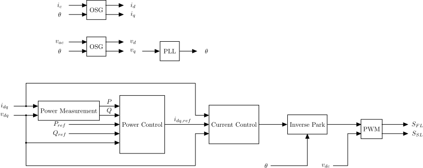
- Perform Clarke and Park transformations.
- Design a PLL for a single-phase grid using an orthogonal-signal generator (OSG).
- Implement a dq-frame power controller and a dq-frame current controller with decoupling terms.
- Decide, for a given application, whether abc or dq control is the better choice.
Prerequisites
To take the course, I recommend a basic understanding of electronics, math, and control theory. I expect that you understand, at a surface level, how inductors and PI controllers work. However, you do not need to understand how an inverter works or how it is controlled. These topics are covered in the course.
Notation (used throughout)
| Symbol | Meaning | Units |
|---|---|---|
| $v_{ac},\ i_c$ | Grid-side voltage and converter output (inductor) current, time-domain | V, A |
| $V_{ac},\ I_c$ | RMS values of the same quantities (capital letters for RMS) | V, A |
| $v_c$ | Converter voltage (the inverter's controlled output) | V |
| $v_{dc}$ | DC-link voltage | V |
| $L_c$ | Output inductance | H |
| $\omega = 2\pi f_{ac}$ | Grid angular frequency | rad/s |
| $\theta$ | Grid voltage angle | rad |
| $\hat{\theta}$ | PLL estimate of $\theta$ | rad |
| $v_\alpha,\ v_\beta$ | Clarke-transformed voltages (stationary) | V |
| $v_d, v_q, i_d, i_q$ | Park-transformed voltages and currents (rotating) | V, A |
| $D_{FL},\ S_{SL}$ | Fast-leg duty cycle, slow-leg gate signal | —, {0,1} |
| $S_{FL}$ | Fast-leg gate signal | {0,1} |
| $P,\ Q$ | Active and reactive power (average) | W, var |
Lower-case letters denote instantaneous time-domain quantities; upper-case letters denote RMS values. Subscript ref means "commanded"; hat ($\hat{\cdot}$) means "estimated".
Control overview
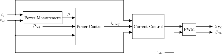
Control Structure in the stationary frame (abc)
Control Structure in the rotating frame (dq)
The Inverter
Topology
A simplified model of a single-phase inverter is shown in Figure 1. On the left is a DC link, and on the right are an AC voltage source and an inductor. In between, we have two switching legs. We use fast leg (FL) and slow leg (SL) to refer to the left and right switching legs, respectively. $S_{FL}$ and $S_{SL}$ are the gate signals for the upper switches. Only one switch can be on at a time in each leg, as indicated by the overline.
The switching legs are called fast and slow because they switch at different frequencies. The slow leg switches at twice the AC voltage source's fundamental frequency. While the fast leg switches at a much higher frequency. The fast-leg / slow-leg switching strategy is well suited for a PFC rectifier and is a natural choice for a bidirectional single-phase inverter. If you design your own inverter, you will pick a switching strategy to fit your goals (efficiency, EMI, device count). The specific PWM choice does not change the current- or power-control design that follows — this course is PWM-agnostic from the next chapter onward. All chapters, except the PWM chapter, are relevant to all types of PWM strategies. However, I will use the names "fast leg" and "slow leg" to distinguish between the two legs during switching.
Assumptions used throughout the rest of the course:
- Switches are ideal (zero on-resistance, instantaneous turn-on/off, no dead-time).
- The DC-link voltage $v_{dc}$ is constant and large enough that over-modulation does not occur (see PWM chapter for the explicit bound).
- The output inductor $L_c$ is linear (no core saturation, no equivalent series resistance).
- The grid is modelled as a stiff sinusoidal voltage source $v_{ac}(t) = \sqrt{2}\, V_{ac}\sin(\omega t)$.
- No measurement or communication delay — every signal is available instantaneously.
- Sampling time $\Delta t$ is much shorter than the slowest controller time constant; discrete-time effects are discussed in the appendix.
These are idealisations. The When to use each method chapter and the appendix revisit them.
Simplified model of the Inverter
We can further simplify the model. If we look at $v_{m,SL}$ in the slow leg, when the upper switch is open ($S_{SL}=0$), $v_{m,SL} = 0$ and when it is closed ($S_{SL}=1$), $v_{m,SL} = v_{dc}$. $v_{dc}$ is reference to ground.
$$v_{m,SL} = \begin{cases} 0, & S_{SL}=0 \\ v_{dc}, & S_{SL}=1 \end{cases}$$We can simplify this expression as:
$$v_{m,SL} = S_{SL}\, v_{dc}$$And we can do the same for the fast leg:
$$v_{m,FL} = \begin{cases} 0, & S_{FL}=0 \\ v_{dc}, & S_{FL}=1 \end{cases}$$ $$v_{m,FL} = S_{FL}\, v_{dc}$$Because the fast leg and the slow leg can be modelled as voltages, we can replace them with controlled voltage sources, as shown in Figure 2. If we set the voltage reference (Ground) between the ac voltage ($v_{ac}$) and the slow leg ($v_{m,SL}$), as shown in Figure 2. We would get Figure 3, where $v_c$ is the converter's output voltage.
$$v_c = v_{m,FL} - v_{m,SL}$$Ground is not shown explicitly: it is a reference and could be placed anywhere.


From Figure 3 onwards, "the inverter" means this equivalent circuit: a controlled voltage source $v_c$ in series with the output inductor $L_c$, feeding the stiff AC voltage $v_{ac}$. Our job as control designer is to pick $v_c(t)$ so that the inductor current $i_c(t)$ follows a reference. The fast leg and the slow leg are the physical actuators that realise $v_c$.
Control Structure
On a high level the control of an inverter looks like this:

The controller is split into three blocks: Power control, Current control, and PWM. Each block operates on a different timescale. PWM is an analog signal, meaning a continuous signal, while the current controller is sampled in microseconds and the power controller samples in milliseconds. The sampling times depend heavily on application, but the sampling time of the current controller is significantly lower than the sampling time for the power controller. Each block can therefore be designed on the assumption that the block below it has already settled, which is a standard and extremely effective simplification.
First, we have the Power Control, which calculates the desired current reference ($i_{c,ref}$) based on the measurements and the desired Power. It is desired that the reference current ($i_{c,ref}$) changes slowly in order not to introduce harmonics. Therefore, the Power Controller can be sampled less often than the other block.
Then we have the Current Control, which calculates the reference voltage ($v_{c,ref}$) for the PWM to achieve the desired current ($i_c$).
This controller does not control the DC-link voltage ($v_{dc}$). Whether the inverter should control the DC-link voltage ($v_{dc}$) depends on the system around the inverter and the primary goals. We do not go into detail on that here; if you want to control the dc-link voltage ($v_{dc}$), you can replace the Power Control with a Voltage Control. The input of the Voltage Controller would be the dc-link voltage ($v_{dc}$) and the desired dc-link voltage, while the output would be the reference current ($i_{c,ref}$), as for the Power Controller. Whether you have a Power Controller or a Voltage Controller does not affect the Current Controller or the PWM. The Voltage Controller works well for unity power factor operations, and where computational simplicity is important.
PWM Strategy
The PWM receives a reference voltage ($v_{c,ref}$) and generates gate signals that drive the inverter. The reference voltage ($v_{c,ref}$) is given by the following equation as described above:
$$v_{c,ref} = v_{m,FL} - v_{m,SL}$$Gate Signal Derivation
Remember that $v_{m,FL}$ and $v_{m,SL}$ are given by:
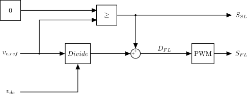
$$v_{m,FL} = S_{FL}\, v_{dc}, \qquad v_{m,SL} = S_{SL}\, v_{dc}.$$Applying the fast-leg gate signal directly is computationally prohibitive: at a 100 kHz switching frequency the outer controller would need to resolve the gate state hundreds of thousands of times per second. Instead we use an average model (also called fundamental-frequency averaging): we compute a duty cycle $D_{FL} \in [0,1]$ — the average of $S_{FL}$ over one switching period — and let an analog comparator turn that into the actual gate signal at the carrier frequency. The slow leg switches only twice per grid period, so its gate signal $S_{SL}$ is kept as-is.
The average-model replacement is
$$v_{m,FL} = D_{FL}\, v_{dc}.$$Substituting into $v_{c,ref} = v_{m,FL} - v_{m,SL}$:
$$v_{c,ref} = D_{FL}\, v_{dc} - S_{SL}\, v_{dc}.$$The unknowns are $D_{FL}$ (continuous, $[0,1]$) and $S_{SL}$ (binary, $\{0,1\}$). Two cases:
- If $v_{c,ref} \leq 0$, choose $S_{SL} = 0$ so $v_{m,SL} = 0$. Then $v_{c,ref} = D_{FL}\, v_{dc}$, but that would force $D_{FL}$ negative when $v_{c,ref}<0$ — impossible. So instead we pick $S_{SL} = 0$ when $v_{c,ref} > 0$ and $S_{SL} = 1$ when $v_{c,ref} \leq 0$, which shifts the fast-leg operating range into a feasible interval.
- Solving the two-case system gives the compact form:
The equation is solvable only when $|v_{c,ref}| \leq v_{dc}$. Outside that range the inverter is over-modulated: the converter simply cannot produce the commanded voltage and the duty-cycle would have to exceed $[0,1]$.
The overall block diagram of the PWM would look like this:
Numerical Example
Drag the sliders to explore the fast/slow modulator. Toggle Show code to see (and edit) the verbatim Python.
That's the first three chapters
The full course continues with chapter 04 onwards: current and power control in the abc and dq frames, the PLL, the Park transform for single-phase systems, and a comparison of the control methods.