The Single-Phase Rectifier
From a diode bridge to an active power-factor-corrected charger.
Introduction
The grid gives you a sine. It swings from $+325\ \mathrm{V}$ to $-325\ \mathrm{V}$ and back, fifty times a second, and averages to zero. A battery wants the opposite: a steady voltage of one fixed polarity. So here is the question this course answers: how do you convert AC into DC? That conversion is called rectification, and the machine that does it is a rectifier.

One way to do it is a diode bridge. Four diodes, arranged so that whichever way the grid is leaning, the current is steered out of the same terminal. The effect is easy to state: the bridge takes the absolute value of the grid voltage. The negative half of the sine is folded up to become positive, and what comes out never reverses. That is DC, in the sense that it has one polarity.
It is not, however, a controlled DC. The output is whatever the grid happens to be doing at that instant, folded; you cannot dial it to the voltage your battery wants. Fixing that is what the rest of this course is about.
Every course so far in this series has moved DC around: the buck stepped a DC voltage down, the boost stepped it up. This one starts somewhere new, with the AC grid on the input side: the 230-volt, 50-hertz sine that comes out of the wall.
It is beneficial to have read the boost guide first, but it is not necessary. We do assume a basic understanding of how a boost converter works — in particular its duty-cycle relation,
$$V_{out} = \frac{V_{in}}{1-D}$$
because the active rectifier in Chapter 4 is a boost converter, and that one formula is where its whole behaviour comes from.
Who this is for
This guide is for anyone who wants to understand how a grid-connected charger turns AC into DC, and why the simplest way to do it is not the way it is actually done in industry. You need a little comfort with basic maths and some basic electronics (what voltage and current are, and roughly what a diode, capacitor, and inductor do). That is it. No prior course in this series is required, and every formula is followed by a plain sentence saying what it means.
A few recurring boxes will help you navigate:
The one thing to remember from a section. If you read nothing else, read these.
A concrete example with real numbers, so the ideas don't stay abstract.
How something is actually done in commercial parts and industry practice, which is often not how the textbook does it.
A short, friendly definition of a piece of power-electronics vocabulary.
A one-line summary at the end of a section or chapter, in case you want the gist before committing to the detail.
Plot figures carry an Open in simulator link. It drops you into the companion web simulator at the matching operating point, where you can change the circuit and re-run it yourself. Use it: seeing a waveform move when you change a component is worth more than reading about it.
The plan
- Chapter 2: why you need a rectifier, and the simplest one there is: four diodes in a bridge, with a capacitor to smooth the output.
- Chapter 3: the trouble with that simple rectifier. It pulls an ugly, spiky current from the grid. We meet harmonics, THD, and power factor, and see why the grid operator does not want this on their network.
- Chapter 4: the fix: the active rectifier, or power-factor-corrected (PFC) rectifier. It is the diode bridge with a boost converter bolted on behind it, controlled so the grid current comes out as a clean sine.
- Chapter 5: how that boost is controlled: two loops, one holding the DC voltage steady, one shaping the current.
- Chapter 6: the version industry actually builds: the totem-pole PFC, which is the same idea with fewer parts.
Everything here is single phase: one live, one neutral, the supply a domestic charger or a small charging station sees. Three-phase rectifiers are a later course.
The running example, and notation
Throughout, we use one running example, with fixed numbers, so nothing stays abstract: a 1 kW charger taking 230 V from the wall and charging a battery through a 400 V DC bus. Every parameter it fixes is in the table below, and the same numbers come back in the duty-cycle plots, the control-loop figures and the worked examples.
| Symbol | Meaning | Value in this guide |
|---|---|---|
| $v_g$ | Grid voltage (the wall) | $230\ \mathrm{V}$ RMS, $50\ \mathrm{Hz}$ |
| $\hat V_g$ | Peak of the grid voltage ($=\sqrt2\cdot 230$) | $\approx 325\ \mathrm{V}$ |
| $P$ | Charger power (our running example) | $\approx 1\ \mathrm{kW}$ |
| $i_g$ | Current drawn from the grid | $\approx 6\ \mathrm{A}$ peak once corrected |
| $V_{dc}$ | The DC voltage we make | $\approx 325\ \mathrm{V}$ (passive) / $400\ \mathrm{V}$ (PFC) |
| $I_{dc}$ | DC current delivered to the battery | $\approx 2.5\ \mathrm{A}$ |
| $f_{sw}$ | PFC switching frequency | $20\ \mathrm{kHz}$ |
| THD | Total harmonic distortion of $i_g$ | high is bad |
| PF | Power factor | we want it near $1$ |
From AC to DC: the passive rectifier
What a rectifier is
A rectifier converts AC voltage into DC voltage. That is all a rectifier is.
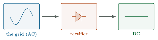
One way to do this is a passive rectifier. A passive rectifier is basically a diode bridge: no transistors, no control, nothing to program, just four diodes arranged in a bridge.
Why we need one
A battery wants DC: a steady voltage of one fixed polarity, plus a controlled current to charge it. The grid offers the opposite: a sine wave that swings from $+325\ \mathrm{V}$ to $-325\ \mathrm{V}$ and back, fifty times a second, averaging to zero. Connect a battery straight to that and it would be charged for half of each cycle and discharged for the other half, net nothing, and the reversing voltage would wreck it.
So the very first thing any grid-connected charger must do is rectify: force that two-way sine into a one-way DC voltage. Everything else in the course is about doing it well; this chapter is about doing it at all.
Four diodes in a bridge
Here is the bridge: four diodes, the grid on the left, the DC output driving the load on the right.
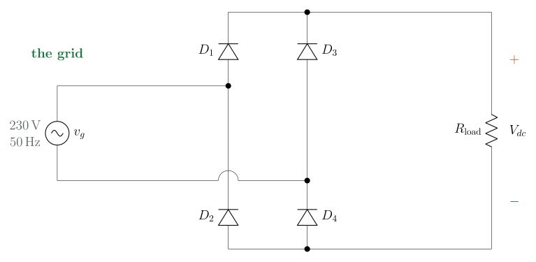
First, how a single diode works. A diode is a one-way valve for current. It conducts only when it is forward-biased: when the voltage across it is positive, meaning its input side is pushed higher than its output side. Push it the other way (input side lower than output side) and it blocks: no current at all. That single rule is everything we need to read the bridge.
Now watch the four diodes steer the grid automatically. Take the positive half-cycle, when the grid's top terminal is higher than its bottom terminal. The grid forces a current out of its top terminal, and that current has to go somewhere. The only forward-biased path is up through the conducting diode ($D_1$): its input side is being pushed higher than its output side, so it conducts. The current is forced up through it because it has no other way to go, since it cannot go down through the reverse diode (that would be the blocking direction). So the current runs out the top, through $D_1$, down through the load, and back out to the grid through $D_4$, while $D_2$ and $D_3$ are reverse-biased and carry nothing.
The green wires and diodes below carry the current; the crossed-out diodes are the ones blocking.
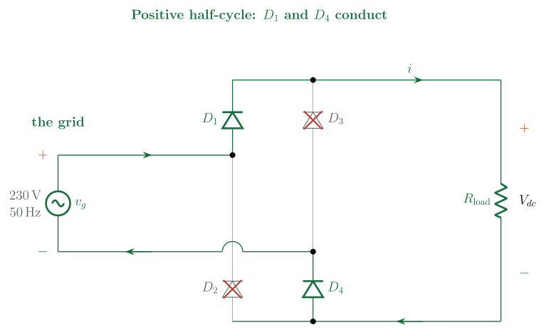
- On the positive half-cycle, the grid pushes current out the top, through $D_1$, down through the load, and back through $D_4$. The other two diodes, $D_2$ and $D_3$, are pushed backwards and block: they carry nothing.
- On the negative half-cycle the grid reverses. Now $D_1$ and $D_4$ block and $D_2$, $D_3$ take over, but notice they route the current through the load the same way as before.
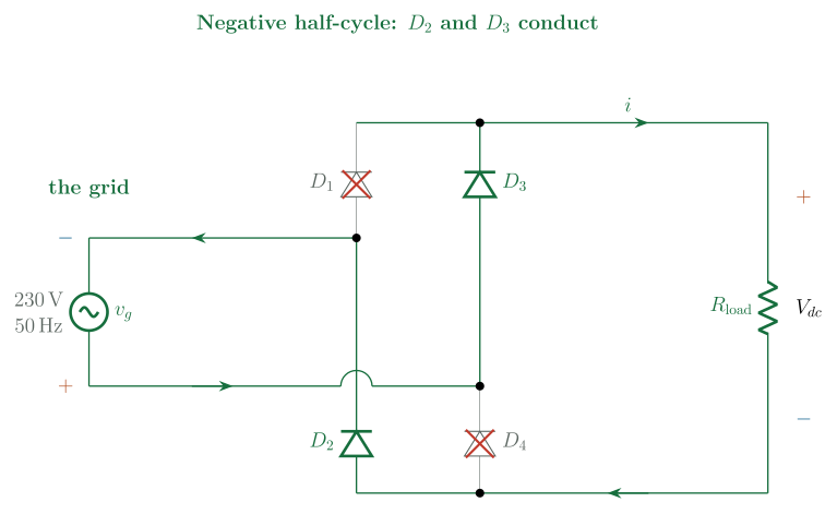
So whichever way the grid swings, the current always leaves by the same DC terminal. The output never reverses. What was a two-way sine becomes a one-way stream of humps: the absolute value of the sine, $|v_g|$. Look at the figure below: the top trace is the grid voltage going in (a sine), and the lower trace is what comes out of the bridge (the same sine with every negative half flipped up).
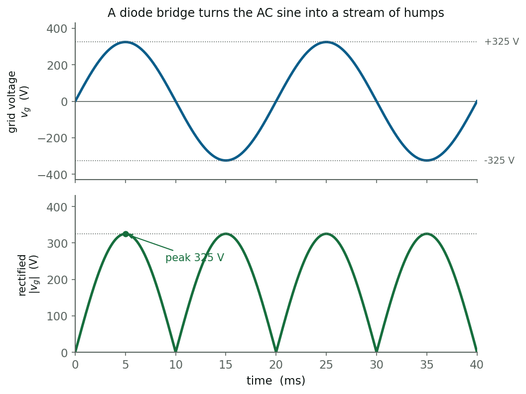
In the lower trace the humps touch zero twice per cycle, once at each grid zero crossing, and that is the signal we now have to flatten.
A full-bridge rectifier uses four diodes to flip the negative half of the AC sine upwards. The output is always one polarity (it never reverses) but it is a train of humps that touches zero twice per cycle, not a steady DC voltage.
Smoothing it: the output capacitor
This is not flat DC yet: it is a train of humps that drops to zero twice a cycle, and a battery (or the DC bus of any electronics) wants a voltage that barely moves. So we add a capacitor to smooth it: hang a big capacitor across the output and it straightens the humps into a near-steady voltage. Let us see how.
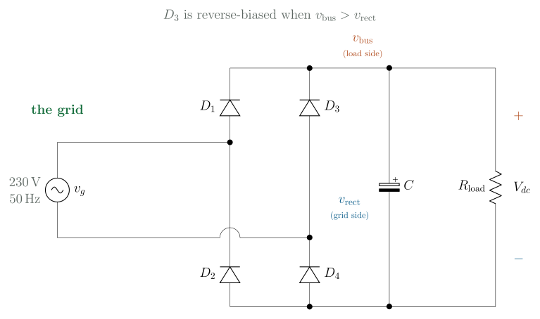
A capacitor resists changes in voltage: think of it as a small reservoir of charge. Each time a hump rises to its peak, it tops the capacitor up to about $325\ \mathrm{V}$. Then, as the hump falls away, the capacitor alone holds the load up, slowly draining until the next peak arrives to refill it.
Why do the diodes stop conducting while the capacitor drains? Reason about it on the circuit. While the capacitor holds the load above the rectified grid voltage, the output side of each diode (the load side) is higher than its input side (the grid side). That is the blocking direction: the diodes are reverse-biased, so no current flows through them. The grid is disconnected, and the capacitor supplies the load on its own. Only when the rising hump climbs back above the capacitor voltage does a diode become forward-biased again, and the grid takes over to refill the capacitor.
A diode is reverse-biased when the voltage across it points the wrong way for conduction: its output side is higher than its input side. A reverse-biased diode blocks: it carries no current. Here it is the capacitor holding the load voltage above the rectified grid that reverse-biases the bridge diodes between peaks.
The result is a DC voltage that sits near the peak (around $325\ \mathrm{V}$), sagging a little between peaks and getting topped back up at each one. That sag is called the ripple.
Using the capacitor equation
To explain how much it sags, and why the current comes back as spikes, we only need one equation, the defining relation of a capacitor:
$$ i = C\,\frac{dV}{dt}. $$The current into a capacitor is its capacitance times how fast its voltage changes. Read it both ways and it explains both halves of the picture.
Voltage droop: between peaks the diodes are off, so the load current $I_{load}$ comes out of the capacitor. Rearranging, $dV/dt = -I_{load}/C$. A bigger $C$ means a slower droop: a flatter voltage, closer to ideal DC.
Current spikes: the capacitor is refilled in a very short window $dt$ near each peak. To restore that charge in such a short time, $i = C\,dV/dt$ must be large: a tall, narrow burst of current.
So the droop and the spikes are two readings of the same equation. Between peaks, $dV/dt = -I_{load}/C$ sets how fast the voltage falls. At each peak, the refill happens in a tiny $dt$, so the current $i = C\,dV/dt$ is forced into a tall spike.

And there is the catch, sitting in the bottom panel. Look at when the grid current flows. The diodes only conduct in the brief window where the rising hump is higher than the drooping capacitor: a short slice near each peak. For the rest of the cycle the capacitor carries the load by itself and the grid current is zero. So the grid is not asked for a smooth sine of current; it is asked for a series of brief, violent gulps.
The capacitor-size tradeoff
Now use the same equation to size the capacitor, and you find a tradeoff with no free side. A bigger capacitor gives a smoother voltage: slower droop, less ripple, closer to DC ($dV/dt = -I_{load}/C$). But a bigger capacitor holds the voltage up longer, so the rising grid takes longer to catch back up, and when it finally does it must replace more charge in a shorter window: a taller, narrower current spike. Smoother voltage, nastier current: the two sides of the same coin.
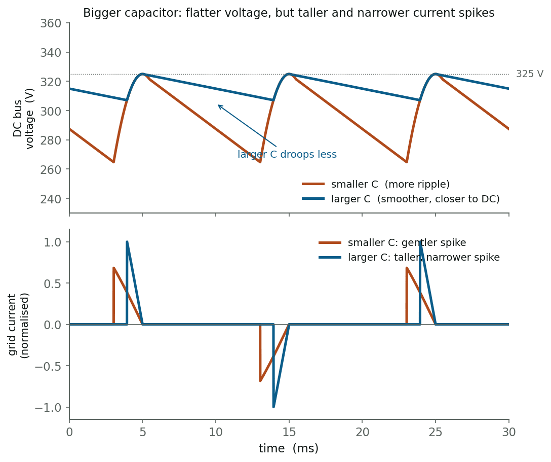
A capacitor across the output flattens the humps into a near-steady DC voltage at about the peak ($\approx 325\ \mathrm{V}$), with a small ripple. But it also forces the grid current into narrow spikes at each peak: the diodes only conduct while the rising sine exceeds the held-up capacitor voltage. A bigger capacitor smooths the voltage further but makes the spikes taller and narrower still.
A passive rectifier (four diodes and a capacitor) is the cheapest way to turn AC into a usable DC voltage, and it is everywhere. But the smoothing capacitor makes the converter draw a spiky, non-sinusoidal current from the grid. The next chapter is about why that is a real problem.
The trouble with the passive rectifier
The passive bridge works: it makes DC. But the spiky current it pulls is a genuine problem. Here is the plain reason it is bad.
Why the spikes are bad for the grid
Ideally, the current a charger draws from the grid should be a clean sine, because that disturbs the grid the least. A sine is a smooth, gentle demand: it asks for a little more current, then a little less, never suddenly.
The capacitor-input bridge does the opposite. It pulls its energy in sudden, narrow spikes: a violent, fast demand on the grid. Asking for that much current that quickly, twice a cycle, is not good for the grid, and not good for the other components sharing it. Those harmonic currents are real currents, and they flow through every wire, transformer and connection between the charger and the power station, doing no useful work, but causing harm along the way:
- They heat the wiring and transformers. Heating depends on the total RMS current, spikes included, so a spiky load wastes capacity and shortens equipment life for no benefit.
- They distort the grid voltage itself. The spiky currents, pushed through the grid's own impedance, bend the voltage sine out of shape, so one bad load degrades the supply for everyone nearby.
- They can excite resonances, unwanted ringing stirred up in nearby wiring or filter components, and add extra stress to a building's shared neutral conductor.
So the concrete problem is simple: pushing short bursts of current is bad for the grid (and probably for everything else connected to it), and a smooth sine would be far gentler. The rest of this chapter puts technical language on exactly how non-sinusoidal the spiky current is, and what that costs. We need three ideas the power industry cares about a great deal: harmonics, total harmonic distortion, and power factor.

A spiky current is many sine waves at once
Here is a fact that does a lot of work, and you have probably met it before. Any repeating waveform, however strange its shape, can be built by adding together pure sine waves: one at the original frequency (the fundamental, here $50\ \mathrm{Hz}$), and others at whole-number multiples of it (the harmonics: $150\ \mathrm{Hz}$, $250\ \mathrm{Hz}$, $350\ \mathrm{Hz}$, and so on). This is the Fourier series: it tells you which frequencies are present in a signal and how dominant each one is. A clean sine is only the fundamental. The more a waveform departs from a sine, the more harmonics you need to build it, and the more its energy sits in the higher harmonics.
The idea that any repeating signal can be written as a sum of sinusoids at the fundamental frequency and its integer multiples. Here we use just one consequence of it: a non-sinusoidal current is a sine at $50\ \mathrm{Hz}$ plus a stack of higher-frequency harmonics, and a current dominated by that stack is far from a clean sine.
Our spiky grid current is about as far from a sine as it gets, so it is rich in harmonics: it is dominated by the higher-frequency components rather than the fundamental.
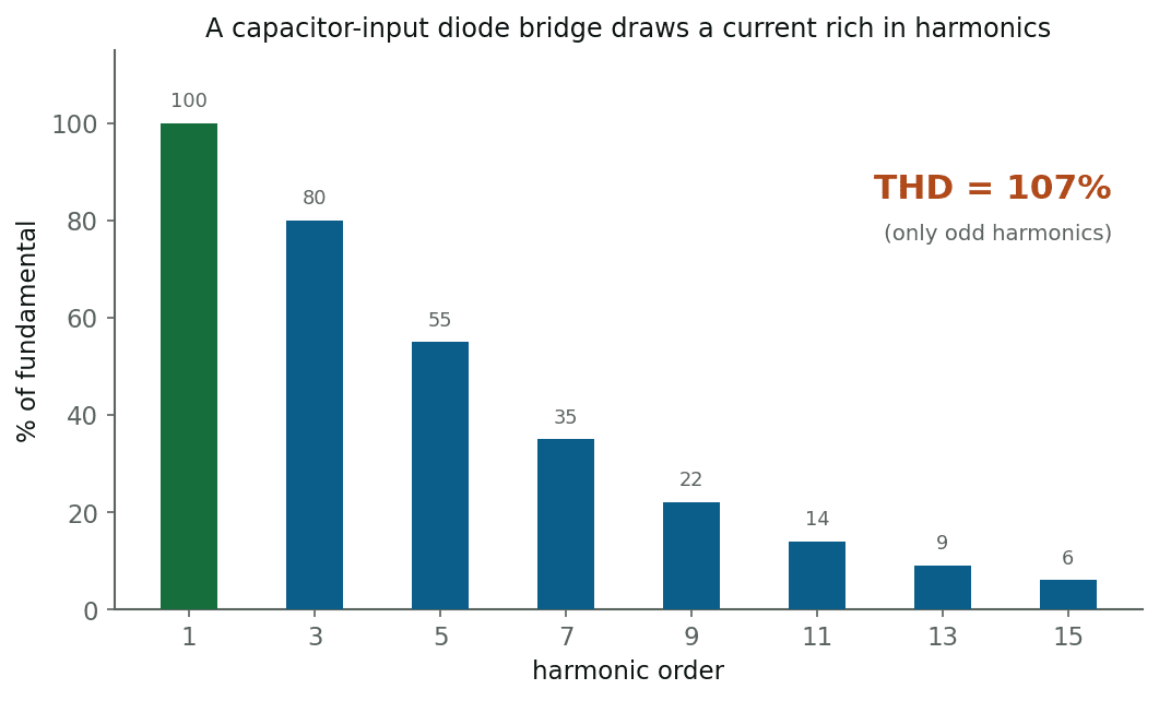
(Only odd harmonics appear: the 3rd, 5th, 7th and so on. That is because the current is symmetric: the negative-half spike is a mirror image of the positive-half spike, and that symmetry cancels every even harmonic. The alternating shape you saw in the last figure is exactly what produces an odd-harmonic spectrum.)
Add the harmonics back one at a time in the figure below and watch the smooth fundamental gradually sharpen into the spike. The more of them you keep, the closer the reconstruction gets, which is another way of saying how much of this current is not the useful $50\ \mathrm{Hz}$ part.
The ideal grid current is therefore a pure sine at the grid frequency, in step with the voltage: only a fundamental ($50\ \mathrm{Hz}$), no harmonics. That is what the grid wants. Then every amp drawn does useful work, and the load looks, from the grid's side, like a simple resistor. Holding the current sinusoidal is half of what the next chapter's circuit is built to do.
Putting a number on it: THD
Now put a single number on how much of that pollution is present, so we can say precisely how non-sinusoidal, how disturbing, a current is. That is the total harmonic distortion, or THD. The more energy sitting in the harmonics relative to the fundamental, the higher the THD.
If $I_1$ is the fundamental current and $I_2, I_3, I_4, \dots$ are the harmonics, then
$$ \mathrm{THD} = \frac{\sqrt{I_2^2 + I_3^2 + I_4^2 + \cdots}}{I_1}. $$
A perfect sine has no harmonics, so its THD is $0\%$. Our diode bridge, with a 3rd harmonic at $80\%$ of the fundamental, a 5th at $55\%$, a 7th at $35\%$ and so on, works out to
$$ \mathrm{THD} = \frac{\sqrt{80^2 + 55^2 + 35^2 + 22^2 + \cdots}}{100} \approx 107\%. $$
The harmonics are larger, added together, than the useful fundamental itself. A regulator typically wants the current THD of a grid-connected charger held to a few per cent, not a hundred.
Active power, reactive power, and power factor
There is a second, related way to describe what the grid has to carry, and it brings in three kinds of power. Active power $P$ is the part that does useful work, measured in watts (W). Reactive power $Q$ describes energy moving back and forth between the grid and the load, with no net work done over a cycle. It is measured in volt-amps reactive (var). Apparent power $S$ is the total electrical loading that the grid equipment must carry, measured in volt-amps (VA).
For sinusoidal voltage and current with a phase shift, these quantities make a right triangle:
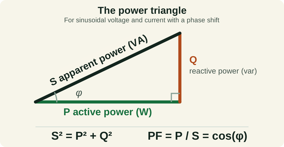
Hold the useful power $P$ fixed and add more $Q$. The hypotenuse $S$ gets longer. At the same grid voltage, that larger $S$ means more current and more capacity are required from the cables and transformers to deliver the same useful power.
The beer glass is a useful follow-up picture for that capacity problem. The beer stands for useful $P$, the foam stands for $Q$, and the whole glass stands for $S$.

When a load draws a sinusoidal current that is perfectly in step with the voltage, its power factor is $1$. If the current leads or lags the voltage, some energy is handed back to the grid during each cycle. That back-and-forth flow still loads the wires even though it does no net work.
For this sinusoidal phase-shift case, the fraction of apparent power that is useful is the power factor:
$$ \mathrm{PF} = \frac{P}{S} = \cos\varphi. $$A power factor of $1$ is perfect: all the supplied power does work. A poor power factor means the grid must push extra current and size its cables and transformers for it to deliver a given number of useful watts.
The glass is a capacity analogy, not a literal construction rule. For a sinusoidal load with a phase shift, the foam represents reactive power $Q$. Our diode bridge is different: its poor power factor comes mainly from distortion, not reactive power. Its current spikes raise $I_{\mathrm{rms}}$ and therefore the apparent power $S$ without raising the useful active power $P$. In that case, read the foam more generally as current capacity that does not become useful power. The distinction matters, and the box below separates the two causes.
The textbook villain is phase shift: current lagging the voltage, the displacement factor $\cos\varphi$. But a diode bridge's current is roughly in step with the voltage; its $\cos\varphi$ is nearly $1$. What ruins its power factor is the second villain: distortion. All those harmonics are current the grid carries but that produce no active power, because active power only comes from the fundamental. So the true power factor is the product of both effects,
$$ \mathrm{PF} = \underbrace{\cos\varphi}_{\text{displacement}} \times \underbrace{\frac{I_1}{I_{\text{rms}}}}_{\text{distortion}}, $$
and for our bridge, with $\mathrm{THD}\approx 107\%$, the distortion term alone is $1/\sqrt{1+1.07^2}\approx 0.68$. Even with the current perfectly in phase, the power factor is stuck around $0.6$ to $0.7$. The harmonics, not a phase shift, are what wreck it.

The passive bridge makes DC, but it is a bad grid citizen: it draws a spiky current with over $100\%$ THD and a power factor around $0.6$ to $0.7$. Those harmonics heat the network, distort the voltage for everyone, and waste capacity. What we want instead is a grid current that is a clean sine, in step with the voltage. Making that happen is power-factor correction.
The active rectifier: a boost PFC
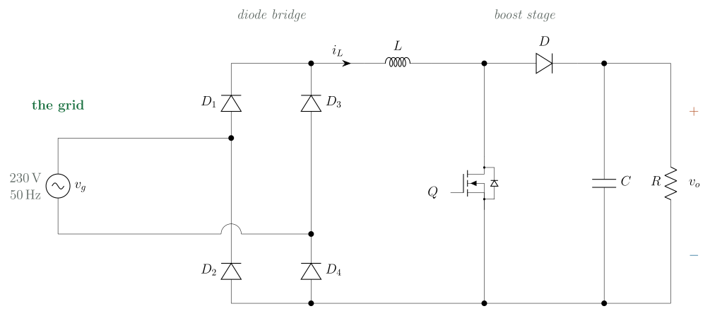
We want the best of both worlds: a steady DC voltage on the output and a clean, sinusoidal current drawn from the grid. A pile of diodes and a capacitor cannot do it: they have nothing to control. We need an active switch and a controller. The standard answer is to take the diode bridge and put a boost converter right behind it. Used this way, the boost is called a power-factor correction stage, or PFC.
What the boost is asked to do here
This is the same boost converter from the boost guide: the same inductor, switch, diode and capacitor, the same step-up action, re-derived from scratch in the average model below so nothing here depends on having seen it before. But it is being asked to do something new, and two differences are worth pinning down.
First: the input voltage is no longer constant. In the boost guide, the input was a steady source (a solar panel, a battery). Here the boost's input is the rectified grid: the train of humps, $|v_g|$, swinging from $0$ all the way up to $325\ \mathrm{V}$ and back, a hundred times a second. The boost has to cope with an input that is constantly moving.
Second: we now care about the input current, not just the output voltage. A normal boost only cares that its output is right; whatever current it draws from its source is incidental. A PFC has the opposite priority bolted on top: its input current must be a clean sine in step with the grid. That is the whole reason it exists.
Here are the two signals that matter most, right up front so you have something to look at: the voltage going into the boost, and the current going into the boost.
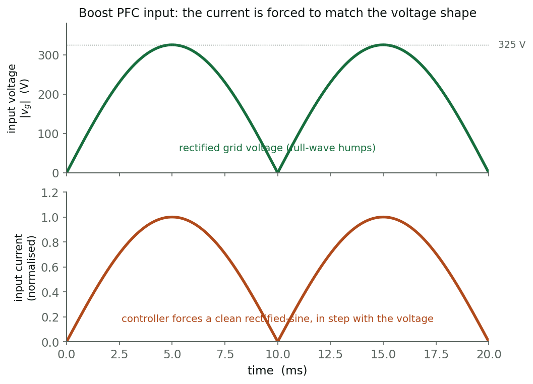
The bottom trace is the prize. Where the passive bridge gulped current in spikes, the boost PFC draws a smooth sinusoidal current that follows the voltage. Seen from the grid, the charger now looks like a simple resistor: THD down to a few per cent, power factor up near $1$. The rest of the chapter is how it manages it.
How a varying input makes the duty cycle move
Recall the boost's voltage rule: with a steady input, the output sat at $V_{out} = V_{in}/(1-D)$, so a fixed input and output meant a fixed duty cycle $D$.
Now feed it the moving rectified input. To hold the output fixed at, say, $400\ \mathrm{V}$ while the input $|v_g|$ swings, the duty cycle can no longer sit still: it must move with the input, instant by instant. Rearranging the boost rule for the duty that holds $V_{dc}$ steady:
$$ d(t) = 1 - \frac{|v_g(t)|}{V_{dc}}. $$When the input is near a zero crossing ($|v_g|$ small), the boost has to step up enormously, so the duty is high, near $1$. At the peak ($|v_g|\approx 325\ \mathrm{V}$, just below the $400\ \mathrm{V}$ output), it barely has to step up at all, so the duty drops to its minimum, $1 - 325/400 \approx 0.19$. Over each half-cycle the duty sweeps from near $1$ down to about $0.19$ and back. For our running example, a $1\ \mathrm{kW}$ charger with this $325\ \mathrm{V}$ peak, that is a grid current peaking at about $6\ \mathrm{A}$ ($P \approx \hat V_g I_{pk}/2$), which is the number we will carry into the control chapter.

A boost can only step up. Its output can never be lower than its input, so $V_{dc}$ must be chosen above the highest the rectified grid ever reaches: above $325\ \mathrm{V}$. That is why a single-phase PFC almost always regulates its DC bus to about $400\ \mathrm{V}$: comfortably above the $325\ \mathrm{V}$ peak, with margin to spare.
Pull the bus target below the $325\ \mathrm{V}$ peak in the figure below and watch the duty hit its floor around each peak: the boost cannot step down, so it loses control exactly there and the current distorts. That is why the bus has to sit at $400\ \mathrm{V}$.
An active rectifier is a diode bridge followed by a boost converter, controlled so it does two jobs at once: hold the DC output steady, and pull a clean sinusoidal current from the grid. The trick is that its input voltage is the moving rectified sine, so its duty cycle has to sweep across every half-cycle: high where the input is low, low at the peak.
The average model: what the controller is designed against
The next chapter builds a controller for this boost, and every equation in it (the feed-forward duty, the plant it is designed against) comes from one short piece of reasoning here.
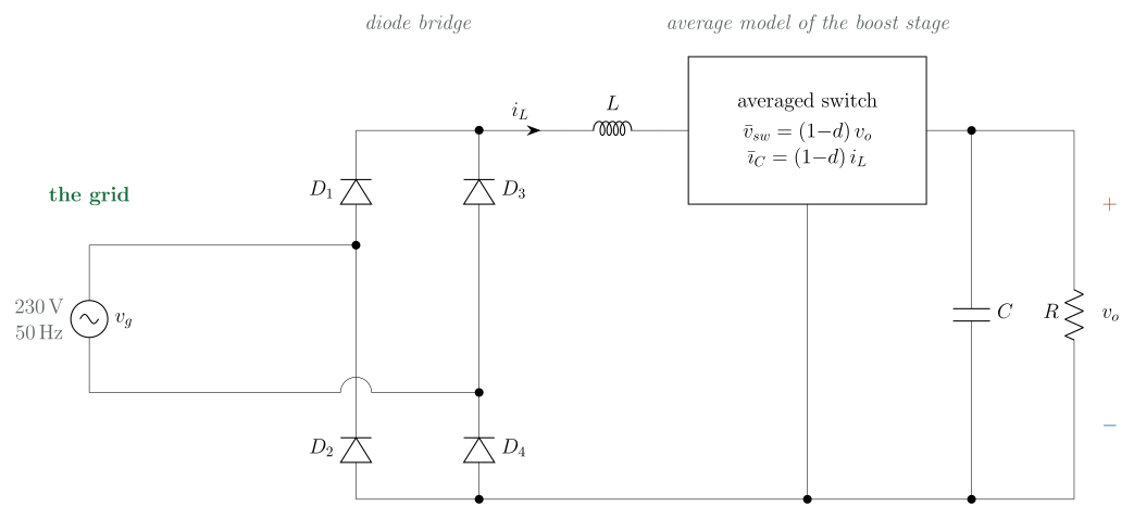
The boost switches on and off tens of thousands of times a second (a few hundred times within each single $20\ \mathrm{ms}$ grid cycle, at our $20\ \mathrm{kHz}$ switching frequency). We do not want to track every switching event to design a controller; we want a smooth model of the average behaviour. The trick is to replace the switch by its duty cycle: instead of a device that is fully on or fully off, treat it as if it applies the fraction $d$ of the time, on average, over each switching period.
Do that, and the inductor sees, on average, the input voltage minus a fraction $(1-d)$ of the output voltage. In steady state the average voltage across an inductor must be zero (otherwise its current would ramp away), so
$$ \langle v_L\rangle = |v_g| - (1-d)\,V_{dc} = 0 \quad\Longrightarrow\quad V_{dc} = \frac{|v_g|}{1-d}. $$That is the familiar boost relation, now written for the moving rectified input. Rearranged for the duty,
$$ d = 1 - \frac{|v_g|}{V_{dc}}, $$which is exactly the duty sweep we plotted above. This averaged relation (the switch replaced by its duty) is the average model, and it is the plant the controller in the next chapter is designed against.
Drawn as a circuit, the average model is the bridge and inductor as before, but with the switch-and-diode pair replaced by a single averaged switch that applies the fraction $(1-d)$ of the output voltage to the inductor side and passes the fraction $(1-d)$ of the inductor current to the output.
Controlling the boost PFC
A boost converter is controlled with two nested feedback loops, an arrangement called cascade control. If you took the boost guide, that structure and the PI controllers inside it are already familiar, and a PFC controller is that same machinery with a couple of extra ideas layered on top. If you have not, nothing here assumes it: the next section builds cascade control from first principles, and every controller block gets opened up and explained in turn.
Why it must be cascade control
A plain boost, feeding a steady load, can be run with a single voltage-mode loop: measure the output, adjust the duty, done. A PFC cannot. It has two things to control at once (the DC output voltage and the shape of the input current) and you cannot regulate two quantities with one loop. So a PFC must use cascade control: an outer loop for the voltage wrapped around an inner loop for the current. There is no voltage-mode-only version of a PFC.
The two loops run on very different timescales:
- The output voltage must be held steady at $400\ \mathrm{V}$. This is slow: the DC bus is allowed to wobble gently across a grid cycle, and we only trim it over many cycles. It is the same outer voltage loop you already know from the cascade boost controller.
- The input current must be shaped into a sine that follows the grid, instant by instant. This is fast: the current has to track the moving reference faithfully within each switching period. It is the inner current loop, again just like the cascade boost.
The overall control structure
The cleanest way into PFC control is the block diagram. Here is the whole controller on one page; we will then open up each controller block in turn and see what is inside it.
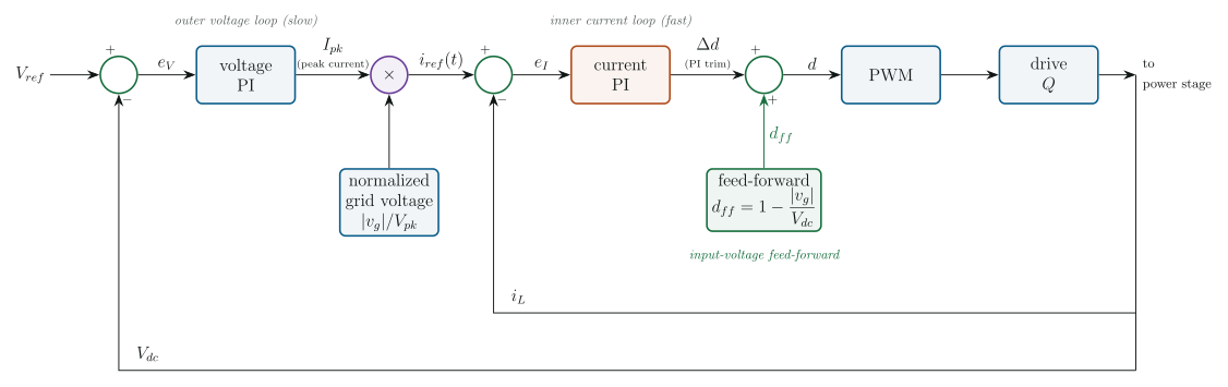
Read it left to right. The outer voltage loop sits on the far left and produces one number, the peak current $I_{pk}$. The multiplier turns that number into a shaped reference $i_{ref}(t)$ by multiplying it with the normalized grid voltage. The inner current loop then drives the inductor current onto that reference, and a feed-forward path supplies most of the duty directly. Two feedback wires run along the bottom: $i_L$ back to the inner loop, $V_{dc}$ back to the outer loop.
So far each controller is a single labelled box. The two boxes that do the real work (the voltage PI and the current PI) hide their internals. The next two sections open them up.
Inside the voltage controller
The outer voltage controller is the simpler of the two. Open the box and there is exactly one job: hold the DC bus at its target by setting the current amplitude. The diagram below is just the voltage loop's insides, lifted out of the overall structure.
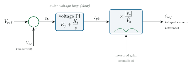
Trace it through. The reference $V_{ref}$ (the $400\ \mathrm{V}$ target) meets the measured bus voltage $V_{dc}$ at the summing node; the node forms the error $e_V = V_{ref}-V_{dc}$. That error feeds a PI controller, and the PI's output is the peak current $I_{pk}$. That is the whole of the loop's regulating machinery: an error and a PI. If the load takes more power the bus sags, $e_V$ goes positive, and the PI raises $I_{pk}$ to refill it; if the bus runs high the PI backs $I_{pk}$ off. The integral term guarantees the bus settles exactly on $400\ \mathrm{V}$ with no standing error.
Notice what the box does not output: any shape or timing. $I_{pk}$ is a bare amplitude. The sinusoidal shape arrives at the multiplier that follows it, where the normalised grid is scaled by that amplitude, which is why the voltage controller can afford to be slow (more on that below).
Inside the current controller
The inner current controller is where the PFC's signature trick lives. Open the box and there are two paths feeding the duty, not one: a feedback PI and a feed-forward computed straight from the grid voltage.
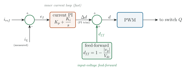
Trace this one too. The shaped reference $i_{ref}$ meets the measured inductor current $i_L$ at the first summing node, forming the error $e_I = i_{ref}-i_L$. The PI acts on that error and outputs $\Delta d$, a small trim, not the whole duty. At the second summing node that trim is added to the feed-forward term $d_{ff}=1-|v_g|/V_{dc}$, which is computed directly from the measured grid voltage. Their sum is the duty $d$, which goes to the PWM and on to the switch.
The feed-forward path (the green branch into the second summing node) is the key idea of this chapter: instead of asking the PI to chase the fast-moving duty on its own, it is given a running start from the model. The next two sections build that duty and show exactly why the PI is still needed on top of it.
With both controllers opened up, we can now walk the parts of the structure in detail: how the current reference is built (the multiplier between the two loops), how the duty is built (the feed-forward plus the inner PI), and why the PI is there at all.
Building the current reference: amplitude times normalized voltage
In a plain boost, the outer voltage loop tells the inner current loop "hold the current at this steady level". In a PFC that is not enough: a steady current would be a flat line, not a sine. The fix is the standard, simple, industry method, and it is worth getting exactly right.
The outer voltage loop compares the DC bus to its $400\ \mathrm{V}$ target and outputs a single number: the peak current $I_{pk}$, the amplitude of the current we should draw. If the load takes more power, the bus sags, and the voltage loop raises $I_{pk}$ to refill it. It is just an amplitude; it carries no shape and no timing.
The shape and timing come from the grid itself. The boost stage sits behind the diode bridge, so what it actually sees is the rectified grid, $|v_g|$: never negative. We take that measured rectified voltage and normalize it (divide it by its peak $\hat V_g$) so it becomes a unit-height template that is exactly the shape of the rectified grid, in phase with it. Then the current reference is simply
$$ i_{ref}(t) = I_{pk}\,\frac{|v_g(t)|}{\hat V_g}. $$Because the template is the measured rectified grid voltage, the current reference automatically follows it in shape and phase, the current tracks the voltage by construction, which is unity power factor. There is no separate sine oscillator to build or synchronize; you reuse a voltage you already measure. (And note: it is the same measured rectified grid voltage that the feed-forward below uses, so this measurement earns its keep twice.)
The outer voltage loop outputs an amplitude, the peak current $I_{pk}$. The current reference is that amplitude times the normalized measured rectified grid voltage, $i_{ref} = I_{pk}\,|v_g|/\hat V_g$. Multiplying by the real (rectified) grid voltage, rather than a synthesized sine, makes the current follow the voltage in shape and phase automatically: unity power factor, for free.
Building the duty: feed-forward does the hard work
Now the inner loop. Here is the single most important idea in PFC control, and it is the one a plain boost usually does without.
In a steady boost, the duty cycle barely moves, so a current PI on its own can hold it. In a PFC the operating point is a moving target: the rectified input $|v_g|$ sweeps from $0$ to $325\ \mathrm{V}$ and back a hundred times a second, so the duty must track it every instant. Asking a PI alone to chase that fast-moving target would leave a large tracking error and a distorted current.
So we do not ask it to. We feed the input voltage forward. From the average model in the last chapter we already know the duty that holds the bus steady for a given input:
$$ d_{ff} = 1 - \frac{|v_g|}{V_{dc}}. $$We compute this directly from the measured (normalized) grid voltage and use it as the base duty. The feed-forward tracks the moving operating point; the current PI supplies only the small residual it misses. This feed-forward is crucial here in a way it is not for a steady boost, and it is what makes the current come out clean.
Why a PI on top of the feed-forward
If the feed-forward already computes the duty, why keep a feedback controller at all? Follow the chain and the answer falls out on its own.
The inner loop controls the inductor current. Across the inductor, $v_L = L\,di_L/dt$, and on average $v_L = |v_g| - (1-d)V_{dc}$. The feed-forward sets $d$ so that this average is nominally zero at the right current: that is the model. But the model is not the whole truth: we do not capture every dynamic, the inductance and the bus voltage are not known exactly, the measurements carry noise, and the load changes. So a proportional-integral (PI) controller sits on the current error $i_{ref} - i_L$ and trims the duty by whatever the feed-forward missed. Its integral term drives the steady-state current error to zero despite the plant uncertainty.
The outer voltage loop works the same way one level up. Its plant is the DC bus capacitor: the bus voltage rises when more charge goes in than the load takes out, and falls otherwise. A PI on the voltage error $V_{ref} - V_{dc}$ sets the amplitude $I_{pk}$ so that, on average, just enough current is drawn to hold the bus. Again the integral term removes the steady-state error that the imperfect model would otherwise leave.
So the division of labour is: the feed-forward handles the known, fast-moving behaviour from the model; the PI loops handle everything the model does not capture: uncertainty, noise, and load changes. A PI is enough here because the reference the inner loop must track is already shaped for it; the PI only has to null a slowly varying residual error.
The voltage loop must be slow
One more point, easy to miss and important. The outer voltage loop must be deliberately slow: its bandwidth well below the grid frequency.
Here is why. The voltage loop's output is the amplitude $I_{pk}$, and the current reference is $I_{pk}\,|v_g|/\hat V_g$. If $I_{pk}$ moved much within a single grid period, it would modulate the reference across the cycle and distort the otherwise-clean sinusoidal current, adding the very harmonics we are trying to remove. The single-phase bus also carries an unavoidable $100\ \mathrm{Hz}$ ripple; a fast voltage loop would try to "correct" that ripple and, in doing so, smear it into the current. So we tune the voltage loop intentionally slow: it should barely change $I_{pk}$ over one grid cycle, trimming the bus only across many cycles. Slow voltage loop, clean current: that is the trade, and it is deliberate.
How it behaves
Here is the controller settling from a cold start, both loops at work, for our running $1\ \mathrm{kW}$ example: the current amplitude settles at the $6\ \mathrm{A}$ peak that example needs, switching at $20\ \mathrm{kHz}$. These first plots are from the average model, the switch replaced by its duty, which is the right tool for seeing the loop behaviour.
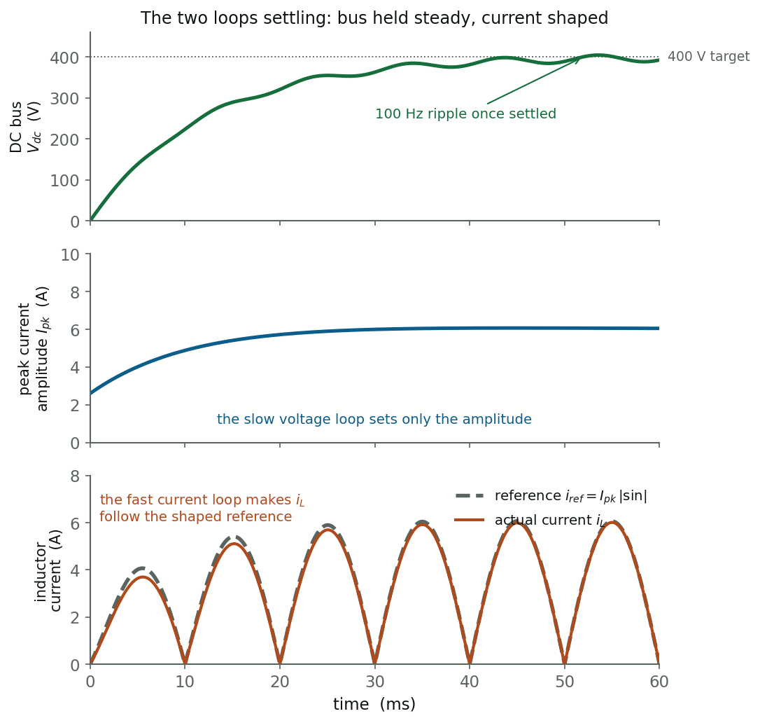
Retune the two loops yourself below. Speed the voltage loop up and you will see exactly the failure the last section warned about: $I_{pk}$ starts wobbling within the grid cycle and the current stops being a clean sine.
The average model is clean because it has hidden the switching. The exact (switching) model shows what the inductor current really looks like: the same shaped sine, but with high-frequency ripple riding on it as the switch chops on and off within each period.

A PFC controller is cascade control: a slow outer voltage loop outputting the peak-current amplitude $I_{pk}$, and a fast inner current loop tracking the reference $i_{ref}=I_{pk}\,|v_g|/\hat V_g$ with the feed-forward duty $d_{ff}=1-|v_g|/V_{dc}$ built above. The voltage loop is kept slow so it does not distort the current.
Controlling a boost PFC is cascade control with two extra ideas: build the current reference as $I_{pk}\times$(normalized grid voltage), and feed the input voltage forward as the base duty so the PI only has to trim. Keep the voltage loop slow. The output stays at $400\ \mathrm{V}$; the grid current comes out a clean, in-phase sine.
The totem-pole PFC
The boost PFC of the last two chapters is the right circuit to learn the ideas on: it made the mechanism plain to see. But it is not, in most modern chargers, the circuit that actually gets built. The totem-pole PFC is where the field has gone, and this chapter shows why: it is the same boost PFC you already understand, with the lossy diode bridge folded away.
Pros and cons, before the mechanism
Before we open the circuit, here is why anyone bothers, and what it costs.
The totem-pole uses just 2 diodes (the slow leg) plus 2 switches (the fast leg): four devices total, against the conventional bridge-plus-boost's 4 bridge diodes + 1 boost diode + 1 switch, six devices total. The efficiency gain comes from the conduction path, not the total count: at any instant the totem-pole's current flows through one slow-leg diode plus one switch, while the bridge-plus-boost's current flows through two bridge diodes plus the boost device. One fewer semiconductor drop in the path means less power is burned as the current passes through, which means higher efficiency. At the efficiencies modern chargers are pushed to, that matters.
The price is complexity. The totem-pole needs a more involved controller (we will see the modulation change below), and it is genuinely less intuitive than the bridge-plus-boost: it takes more work to convince yourself it even is a boost. More efficient, but harder to understand and to control.
Now the circuit.

Read the topology off the figure. The boost inductor $L$ sits in series with the grid, the same energy-storing element doing the same job as before. One leg is the fast leg: two switches ($Q_1$, $Q_2$) chopping at high frequency to shape the current, the boost action. The other leg is the slow leg: two diodes ($D_a$, $D_b$) that simply steer the polarity, conducting for a whole half-cycle at a time at $50\ \mathrm{Hz}$. That is the whole device count: two switches, two diodes, one inductor.
Proving it is a boost PFC
The claim is that this is a boost PFC, just folded up. We will prove it the same way we read the passive bridge: cross out what is not conducting, then rearrange what is left into a shape you recognize. Two steps per half-cycle.
Positive half-cycle
When the grid voltage is positive, the current is forced down through the slow leg's conducting diode (it has no other path) while the other slow-leg diode is reverse-biased and irrelevant. Cross it out.

Now rearrange. The conducting diode, while it is on, is just a wire: a short. Redraw the remaining circuit with that diode as a plain connection, and the inductor, the fast-leg switch and the output capacitor fall into the exact layout of a boost converter.

Negative half-cycle
The negative half is the same idea, with the other slow-leg diode conducting. Cross out the now-irrelevant one and force the current through the conductor.

Rearrange again, and this time reach for the reason it comes out the same, rather than just trusting that it does. The totem-pole's fast leg ($Q_1$ on top, $Q_2$ on bottom) and slow leg ($D_a$ on top, $D_b$ on bottom) are built as mirror images of each other about the horizontal midline. Reversing the grid polarity is exactly a top-bottom flip of that mirror: the diode that was irrelevant a moment ago ($D_a$) now conducts, the one that was conducting ($D_b$) is now irrelevant, and the two switches swap which one plays the boost switch and which one's body diode (the diode every MOSFET carries built in) plays the boost diode. Because the circuit itself is symmetric under that flip, retracing the same two steps, short the conducting slow-leg diode, then redraw, lands on the identical inductor-switch-diode-capacitor loop, with $Q_1$/$Q_2$ and $D_a$/$D_b$ simply having traded places.

So the totem-pole is a boost converter that swaps which devices play the boost role each half-cycle. The bridge's four diodes are gone, replaced by a slow leg of two diodes and a fast leg of two switches: fewer parts, and the current no longer pays a two-diode bridge toll on every pass: it now flows through a single slow-leg diode instead of two series bridge diodes. That is the efficiency win.

The controller difference
If the power circuit is a boost both halves, the control is the boost PFC control too: cascade loops, the current shaping $i_{ref}=I_{pk}\,|v_g|/\hat V_g$, the input-voltage feed-forward, all of it carries over unchanged. There is exactly one difference: a half-cycle-dependent modulation.
On the positive half, the fast leg behaves normally, with duty $d$. On the negative half, the polarity through the leg has flipped, so we drive the fast leg with $(1-d)$ instead of $d$. This is the fast-leg / slow-leg PWM idea: the slow leg defines which half-cycle we are in, and the fast leg uses $d$ or $1-d$ to match it. Everything else (the cascade structure, the current shaping, the feed-forward) is identical to the boost PFC.

Device selection for the fast leg, the handover between the two legs right at the zero crossing, and the modern wide-bandgap switches that made the topology practical are the practical refinements a production design adds on top of what is taught here. The thing to carry away is the family resemblance: a totem-pole PFC is a boost PFC with the diode bridge folded into a slow leg, plus a $(1-d)$ flip on the negative half. Everything you learned about shaping the current and holding the voltage still applies.
The totem-pole PFC is the industry-standard single-phase active rectifier. It is the boost PFC with the lossy diode bridge replaced by a slow diode leg and a fast switching leg: fewer semiconductors, higher efficiency, at the cost of more complex control. Both half-cycles are a boost; the only control change is using $(1-d)$ on the negative half. Aside from that modulation, all its behaviour is identical to the boost PFC.
In a sentence
To charge a battery from the grid you must turn AC into DC. The cheap way (four diodes and a capacitor) works but pulls a spiky, harmonic-rich current with a poor power factor that pollutes the grid. The good way is an active rectifier: a boost converter behind the bridge, controlled so it holds the DC voltage steady and draws a clean sinusoidal current in step with the grid. Control it with the cascade boost controller plus a $|\sin|$ multiplier; build it, in the end, as a totem-pole: a boost PFC with the bridge folded in.
You now have the whole arc: why a bare diode bridge spikes the grid current and drags the power factor down, how a boost converter placed behind that bridge turns those spikes into a clean sine by sweeping its duty cycle across every instant of the grid cycle, how to control it with a cascade of a slow voltage loop and a fast current loop plus input-voltage feed-forward, and how the totem-pole folds the diode bridge into the boost itself for fewer parts and higher efficiency.
Play with the same running example in the companion passive-bridge and boost-PFC simulators: watch the spikes grow as the capacitor gets bigger, then switch to the active rectifier and watch those spikes pull back into a sine while the bus holds $400\ \mathrm{V}$ through every corner of the cycle.